It is a pn junction diode which emits light when activated. The surface-mount type in which electrodes are formed on a silicon wafer and then the LED chip is attached to the wafer.

Main Process Steps For High Power Led Manufacturing Download Scientific Diagram
And you can fabricate the LED chip using your fabrication equipment for different application such as nano optoelectronics research.

Led wafer fabrication process. These two areas have been introduced before and semiconductor wafer fabrication techniques of GaN and SiC for optoelectronic devices will be discussed in the following part. Definition of LED wafer. Definition of LED wafer.
4 When a suitable voltage is applied to the leads electrons are able to recombine with electron holes within the device releasing energy in the form of photons. At the beginning of the production process the bare silicon wafer is covered with a thin glass layer followed by a nitride layer. First of all lets start the semiconductor wafer fabrication process steps with luminescence.
Alternately there can be a buffer layer as an intermediate layer between sapphire and GaN epilayersii Contacting the GaN LED structure with adhesive or by metal layers to the conductive. I growth of GaN layer by HVPE MOVPE or MOCVD. Semiconductor Wafer Fabrication in Terms of Luminescence.
The tools and techniques can be enormously expensive and quite complex. The fabrication of GaN VLEDs by wafer bonding and Lift-off process has few basic steps. It is a multiple-step sequence of photolithographic and chemical processing steps such as surface passivation thermal oxidation planar.
Für dieses Detail GaAs-Wafer-Spezifikationen LED besuchen Sie bitteGaAs Epi-Wafer für LED. The wafer fabrication process is one of the most complex and precise manufacturing operations in all the world. Semiconductor device fabrication is the process used to manufacture semiconductor devices typically the metaloxidesemiconductor MOS devices used in the integrated circuit IC chips that are present in everyday electrical and electronic devices.
The pattern is used to modulate light and transfer the pattern through the process of photolithography which is the fundamental process used to build almost all of todays digital devices. There are standardized techniques used throughout the industry though. What we offer is bare LED epi wafer or not processed wafer without lithography processes n- and metals contacts etc.
What we offer is bare LED epi wafer or not processed wafer without lithography processes n- and metals contacts etc. There are two categories of silicon-wafer-based WLP LEDs. And you can fabricate the LED chip using your fabrication equipment for different application such as nano optoelectronics research.
This effect is called electroluminescence and the. Der auf GaN Galliumnitrid basierende LED-Epitaxiewafer von PAM-XIAMEN ist für die Anwendung von blauen und grünen Leuchtdioden LED und Laserdioden LD mit ultrahoher Helligkeit vorgesehen. Slicing the wafers to be used in the fabrication of integrated circuits is a procedure that requires precision equipment.
For these detail GaAs LED wafer specsplease visitGaAs Epi Wafer for LED. And the cavity type in which cavities are formed prior to the electrodes 6. A light-emitting diode LED is a two-lead semiconductor light source.
The glass layer is formed by exposing the silicon wafer to oxygen at temperatures of 900 degrees C or higher for an hour or more depending on how thick a layer is required. Generally the cavity is fabricated using KOH wet etching on a 100 silicon wafer. Adopting the structural manufacturing LED by the GaNP heterostructure lattice matching one formation LED epitaxial structure and eliminating the need for removal of GaAs substrate wafer bonding and transparent substrate complex processes.
The wafers need to be subjected to a number of steps known as lapping polishing and chemical etching. The object is to produce slices that are perfectly flat and as smooth as possible with no damage to the crystal structure.
Semiconductor Today
![]()
Wafer Scale Rbg Microleds Simplify Transfer Process
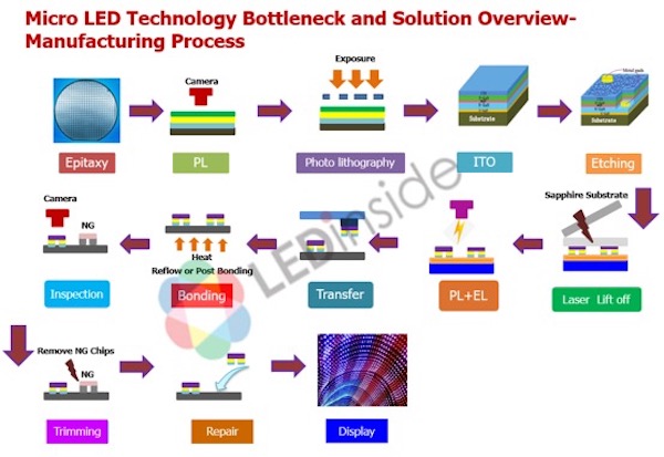
Micro Led Manufacture Process Introduction And Difficulties Analysis Ledinside

Schematic Of Flexible Led Procedures A Epistructures B Chip Download Scientific Diagram

Schematic Diagram Detailing The Fabrication Process A Led Wafer B Download Scientific Diagram

Schematic Of The Fabrication Process Of The Hybrid Rgb Leds A The Download Scientific Diagram

Schematics Of The Fabrication Process Of The Gan Based Blue Led Chip Download Scientific Diagram
![]()
Wafer Scale Rbg Microleds Simplify Transfer Process

Improved Silicon Substrate Leds Address High Solid State Lighting Costs Use Arduino For Projects

Process Flow For Led Manufacturing Download Scientific Diagram
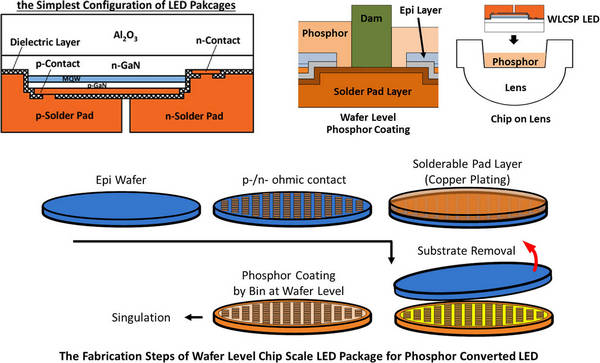
Wafer Level Chip Scale Led Package Jumping Over Flip Chip Csp Led Ledinside
![]()
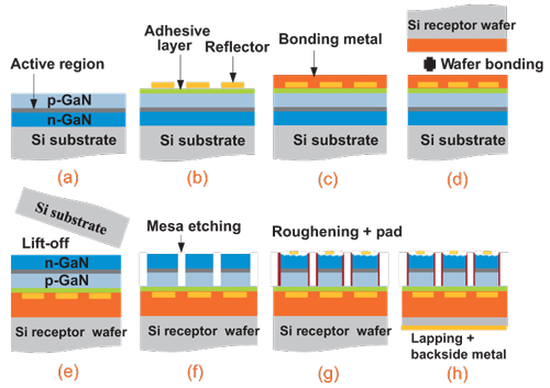
Main Process Steps For Substrate Transfer Process Of Gan Led On Si 111 Download Scientific Diagram
Https Compoundsemiconductor Net Article 104784 Mastering The Manufacture Of Microled Micro Displays

Mled Fabrication A Fabrication Process Of The Mled Probe Shown Across Download Scientific Diagram